The photovoltaic panels generate a direct electrical current. An inverter is needed to connect them to the electrical grid, which provides an alternating current to consumers. This conversion step leads to energy losses that can be minimized with new components.
Large ground-mounted photovoltaic plants as well as plants installed on tertiary or industrial buildings are equipped with "centralized" or "string" inverters and connected to the three-phase electrical grid.
For domestic installations, the available electrical network is single-phase and low voltage. Photovoltaic panels installed on roofs are potentially subject to more shading, leading to losses. Therefore, it is interesting to associate an inverter to each photovoltaic panel allowing an independent operation between modules, an optimal unit yield and very modular operations (easy replacement). This type of inverter, with a power of 200 to 500 W, is called micro-inverter. It is installed on the back of each panel.
This equipment uses key components: power semiconductors.
The CEA at INES is developing new generation inverters to reduce cost, improve energy performance and support the power grid. The compactness of these objects is also an issue in order to control the impact on the installation and maintenance costs of power plants, and to minimize the use of materials.
Our research focuses on electronic architecture and uses "large gap" semiconductors such as silicon carbide (SiC) and gallium nitride (GaN), in particular those developed in the CEA-Leti laboratories in Grenoble.
GaN technology is one of the so-called "wide-gap" technologies (broadband semiconductors), which push the limits of power semiconductors using silicon. It allows for miniaturization and increased energy efficiency while reducing costs. The photovoltaic and automotive industries (with electric vehicles) are the main growth drivers for these new converters based on GaN or SiC semiconductors.
CEA-Leti has state-of-the-art epitaxy (600V and 1200V) and technology to produce GaN 600V diodes and power transistors that outperform silicon equivalents. With this coplanar technology, it would be possible to make the power component "smarter" with protection (temperature, voltage, current, etc.) and control (driver) functions. It is also possible to design bidirectional voltage interrupters which do not exist at present.
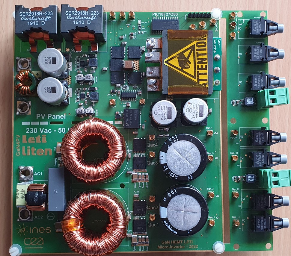
400W photovoltaic microinverter
The CEA at INES has built a high-temperature dynamic characterization bench for these new GaN transistors, as well as the first prototype of a 400W photovoltaic microinverter using the transistors made by CEA Leti's Components Department. This microinverter consists of two conversion stages:
- A DC/DC stage comprising 5 GaN 100V transistors
- A DC/AC stage comprising 4 GaN 650V transistors
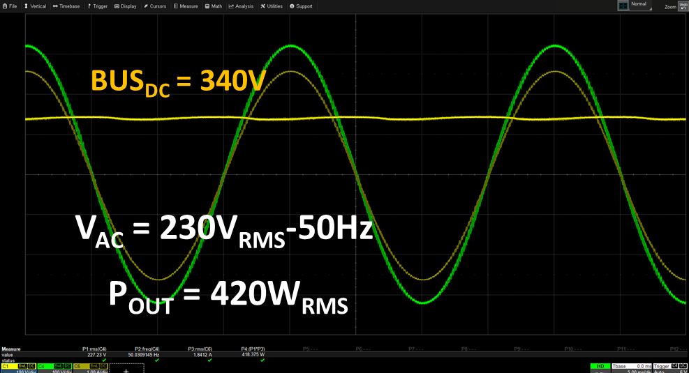
The micro-inverter delivers 420W under 230 V-50Hz with an intermediate DC bus set at 340V.
A second generation of microinverters is planned for the end of 2022, using optimized GaN transistors. Other sizes of inverters will also be targeted in order to prove the concept on higher powers.
This technology is expected to reach the market by 2025-2027. In the meantime, researchers at CEA-Leti and CEA-Liten at INES will improve the technology and develop an integrated digital control system. The team will unveil new prototypes in the coming years.
This work is the subject of patents and several articles and presentations at international conferences (PCIM, EPE).
Références :
[1] A. Bier, V. S. Nguyen, S. Catellani, and J. Martin, "Control of a two-stage, single-phase grid-tied, GaN based solar micro- inverter," EPE2020
[2] N. V. Sang, A. Bier, R. Escoffier, S. Catellani, J. Martin, and C. Gillot, "A high precision dynamic characterization bench with a current collapse measurement circuit for GaN HEMT operating at 175°C," p. 8. PCIM 2021
[3] V. S. Nguyen, S. Catellani, A. Bier, J. Martin, H. Zara, and J. Aimé, "A compact high-efficiency GaN based 400W solar micro inverter in ZVS operation," PCIM, 2020.
[4] V.S NGUYEN, R.ESCOFFIER, S.CATELLANI, M.FAYOLLE-LECOCQ,J.MARTIN "Design, implementation and characterization of an integrated current sensing in GaN HEMT device by using the current-mirroring technique" EPE 2022